Directing Self-Assembly: In Materials Science and Engineering (MSE) the goal is to develop materials with new, often multiple, properties buy using processing techniques to modify their structure. In the early days of MSE, interest was concentrated on ‘microstructure’ – micrometers being a typical size for grains in metals, where the interest was mainly on mechanical properties, and also for ‘microelectronics,’ where the interest was in devices with controlled electronic properties. The last two decades have seen the focus in MSE shift to self-assembly of atoms or molecules into nanometer scale structures in which electron confinement effects and plasmonic behavior emerge. In the future, I expect that artificial materials will be structured according to a hierarchical series of length scales – analogous to biological systems – with different functionalities emerging at each scale. The next step beyond nanotechnology, as suggested by a recent BESAC study, will be learning how to assemble nanostructures into ‘mesoscale’ (10s to 100s on nm) assemblies.
My group has been investigating a hybrid, combination top down/bottom up approach toward getting around the spatial resolution vs. fabrication time bottleneck (direct-writing techniques are intrinsically slow) in achieving mesoscale assembly nanostructures. Most of our studies have been in a simple, prototypical system: molecular beam epitaxial (MBE) growth of GaAs on patterned GaAs (001) substrates. This work exploits the spontaneous formation of nm-size multilayer islands during growth in the presence of an additional diffusion barrier at step edges, the Ehrlich-Schwoebel barrier, by which atoms which land form the vapor, onto an existing island tend to get trapped – and result in the nucleation of next layer islands as additional atoms from the vapor join them. We find that imposing a pre-existing, lithographically defined topographical pattern allow us to direct the self-assembly of these mounds, and that the temperature variation of the ‘natural mound separation’ results in a well-defined series of higher order commensurate mound assemblies. At relatively low growth temperatures the mound density exceeds the density of lithographically defined features – a sort of spatial frequency amplification.
One approach to making and characterizing such structures involves using the scanning tunneling microscope to manipulate or deposit small numbers of atoms. We’ve used the technique of evaporating a thin film of gold or aluminum onto our STM tip, and then applying a voltage pulse between sample and tip to produce nanometer-scale dots of metal on a silicon surface. We then used the same tip both to image the resulting dots, and to measure the local density of electronic states. Although the size- and position-control afforded by this approach are superb, this sort of ‘direct-write’ approach is intrinsically slow, and unlikely to meet the demand of macroscopic arrays of nanometer scale structures called for in practical applications. On the other hand lithographic approaches suffer from insufficient resolution to produce the nanometer scale structures we are interested in. Technology is thus turning to self-assembly to combine small size and large numbers of structures.
Self-organization in nature often leads to pattern formation at characteristic length scales, a phenomenon, which has long fascinated scientists. It also presents a clue as to how bottom-up fabrication of densely packed arrays of nanometer scale devices might be achieved practically. The general idea is to use a template to direct the assembly that occurs during subsequent deposition or growth. Fabrication of the template typically involves either spontaneous pattern formation arising from a balance between thermodynamic driving forces and kinetic processes, or lithography followed by etching to produce artificially patterned substrates. The first approach is relatively simple and clean to carry out, however the characteristic length scales of the patterns, which form are determined mainly by material properties, resulting in a limited range of variation. The second approach is labor intensive, particularly if the detailed structure of individual cells within the pattern is to be controlled.
Research in Directed Self-Assembly: Teaching Nature How to Build
Alternatively, a third, hybrid approach can be used, with an initial lithographically determined pattern setting conditions for the physical driving forces which control evolution during a subsequent sample processing step, i.e. directed self-organization, in which a template is fabricated to guide nature in deciding how to assemble very large numbers of structures quickly. To make this practical, it is crucial to understand the interactions between the underlying physical mechanisms involved, and in particular how these interactions vary with lateral length scale. Some of the recent directions of the research carried out by my group has been toward gaining such an understanding, by probing the effect of the characteristic template length scale in directed self-organization during growth and annealing of semiconductor surfaces.
We start with a template, which we define in a number of different ways-lithography followed by etching, and ‘nanoscraping’ are two approaches we have used; nanoimprint is another possible, and scalable approach. The first relies on depositing a ‘resist,’ usually a polymeric film onto a surface, and then selectively changing the properties of the regions to be removed or left in place. This can be done by irradiating it through a mask with UV light, or irradiating selected regions via a scanned electron beam-both change the resistance of the polymer to being washed away by a chemical developer. Nanoscraping uses an atomic force microscope to selectively scrape away resist; and allows for extremely small patterns to be made. In both approaches the surface, parts of which are covered with resist, others bare, is exposed to a plasma which etches away the top layers. Finally the resist is removed chemically, leaving a clean but topographically patterned surface, a template. Our templates typically made up of arrays of cells, with the pattern lateral size and spacing varied systematically from cell to cell. In this way we are able to measure the lateral size dependence quickly, and under otherwise uniform conditions during such processes as epitaxial growth, annealing and reactive ion etching.
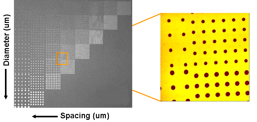
Fig. 1. Patterned GaAs(001) surface containing arrays of cylindrical pits, 50 nm deep, with varying diameter and spacing.
The beauty of this approach is that many patterns can be explored simultaneously, allowing the effect of the pattern length scale to be explored. An example is shown in Figure 1, where we have defined pits of varying diameters and spacings onto a gallium arsenide surface. We now grow more GaAs onto this template, and observe the effect of the length scale on how new structures self-assemble during growth. We find that large period structures amplify during growth: the pits effectively grow deeper, while those whose period is below a certain characteristic size relax during growth. This characteristic size moves to larger values as we grow thicker films, and so eventually even large period structures relax, but the surface shows a transient instability. We’ve explored the temperature dependence, and find that the nature of the instability changes beneath ~540 C; rings of material form around pits during growth beneath this. We explain this change based on competing kinetic effects: one is associated with a barrier that atoms feel on diffusing across a step from above, which is important at low temperatures. The second is a faster collection of atoms by larger terraces, important at high temperatures. In more recent work, we have extended our patterns downward to mesoscale (10s and 100s of nanometers) dimensions.
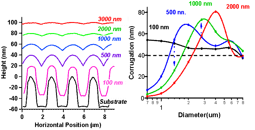
Fig. 2. (Left) Atomic Force Microscopy Height profiles across patterned GaAs(001) for 1 um pits spaced at 2 um, vs. thickness of grown film, (Right) with varying diameter and spacing. (right) Measured peak-valley height of patterns vs. initial diameter for different grown thicknesses. Pattern lengths larger than the peak value amplify, those beneath it decay.
In related experiments, we have patterned stepped silicon surfaces, and measured how the length scale of our pattern affects the self assembly of bunches of steps during heating in vacuum. Beneath a characteristic length scale bunches of straight steps form, while above this the bunches form near sinusoidal shapes, with the waviness of the bunches decaying at the same rate as the height. This length scale is set both by the stiffness of the steps and their interactions. Using a simple model in which steps move across the surface in response to these effects and sublimation we’re able to reproduce the pattern size dependence of the self-organization of bunches of steps during annealing. (Click here for a (347 MB !) movie showing the relaxation for the smallest period structure)
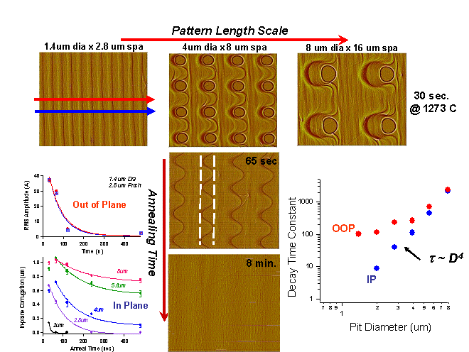
Fig.3. Self assembly of straight step bunches during annealing of short period patterned stepped Si(111), but wavy step bunches for long period patterns. The decay times for step bunch waviness (IP) and height (OOP) are different for small periods, but converge for large pattern structures.
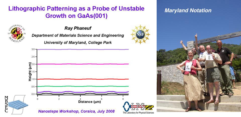
I presented some of our results on patterning for directed self-organization at the recent “Nanosteps: Self-organized nanostructures on crystal surfaces” Workshop (http://www.im2np.fr/nanosteps/NanoSteps.html ) in Cargese, Corsica. At left: Ellen Williams (Y), Ted Einstein (X) and John Weeks (Z) illustrate the “Maryland Notation” for directions on stepped surfaces. Also pictured is Alberto Pimpinelli (waving).